SENSOR TECHNOLOGY AND
DESIGN
| | |
|
Power over
the
1-Wire
Net
The 1-Wire fusion of network connection and
power offers great economy, but the question of how to provide energy for
the occasional indicator or sensor must be addressed.
Dan Awtrey, Dann EL Associates
The 1-Wire net is an
economical bus based on an open-drain master/slave multidrop architecture
that uses a resistor pull-up to a nominal 5 V supply at the master. The
net contains three main elements: the bus master, wiring and associated
connectors, and 1-Wire slaves. The protocol uses conventional CMOS/TTL
logic levels with operation specified over a supply voltage range of 2.8�E
V. Master and slaves are configured as transceivers, allowing
bit-sequential data to flow in either direction, but restricted to one
direction at a time, with data read and written least significant bit
first. Data are transferred with respect to time slots; to write a logic
one to a slave, for example, the master pulls the bus low for  15 µs. To write a logic zero, the master pulls the bus
low for at least 60 µs to provide timing margin for worst-case conditions.
A system clock is not required, as each slave is self-clocked by its own
internal oscillator synchronized to the falling edge of the master. Power
for slave operation is derived from the bus during idle communication
periods when the data line is at 5 V. Except for a software-controlled 15
mA strong pull-up used to accelerate the rising edge of a time slot, only
5 mA is normally available on the net. It is this limit that hinders the
powering of indicators and sensors. The energy supply problem can be
solved in any of four ways, all of which take into account the amount of
energy required and for how long, as well as to the distance from its
source to the bus master: 15 µs. To write a logic zero, the master pulls the bus
low for at least 60 µs to provide timing margin for worst-case conditions.
A system clock is not required, as each slave is self-clocked by its own
internal oscillator synchronized to the falling edge of the master. Power
for slave operation is derived from the bus during idle communication
periods when the data line is at 5 V. Except for a software-controlled 15
mA strong pull-up used to accelerate the rising edge of a time slot, only
5 mA is normally available on the net. It is this limit that hinders the
powering of indicators and sensors. The energy supply problem can be
solved in any of four ways, all of which take into account the amount of
energy required and for how long, as well as to the distance from its
source to the bus master:
- Sourcing power whenever the line is above 3.5 V
- Sourcing power by transferring charge to a capacitor through a
blocking diode
- Sourcing power with the strong pull-up during idle communication
time
- External power source using spare conductors in the cable
Because 1-Wire slaves are designed to operate off a single
lithium cell, the energy available between supply levels of 3.5 and 5 V
can be tapped. This is equivalent to operating the load in shunt mode and
may be used to operate clamp-type loads such as LEDs. This
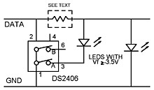
Figure 1. Whenever the output of the
DS2406 is pulled low, the LED is on and the voltage on the bus
is ~3.5 V, for forward voltage of the LED.
| | requires that the
total voltage drop across the LED(s) be at least 3.5 V to allow sufficient
noise margin for reliable communication. While it is possible in certain
installations to connect the shunt load permanently across the bus, the
load should generally be operated under bus master control by connecting
it between 1-Wire DATA and the output of an addressable switch (see Figure
1). In this mode, 1-Wire communication takes place below 3.5 V and power
delivery occurs above that value. Whenever the output of the DS2406 is
pulled low, the LED is on and the voltage on the bus is ~3.5 V, the
forward voltage of the LED. When the output is turned off, the LED is off
and the bus voltage is at its nominal 5 V value. Operational current is
supplied by the bus master, which for the DS2480-based DS9097U com port
adapter is limited to ~5 mA during normal communications but can be
increased to ~15 mA with a software-controlled strong pull-up during
intervals when there is no communication activity. As shown in Figure 1,
the bus voltage will be clamped to a level that keeps the active pull-up
on and supplying 15 mA. If this is not acceptable, a current-limiting
resistor (dotted box) shown connected between the data line and the LEDs
will allow the active pull-up to turn off. �The LINK�Eand other bus master
circuits are capable of supplying more power than the DS2480 [1].
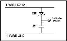
Figure 2. A Schottky diode and
capacitor across the bus generate a local supply on the net at
a point of interest.
| | For some
applications, it may be acceptable to use a series Schottky diode and a
capacitor across the bus to generate a local supply on the net at the
point of interest (see Figure 2). In its wind speed sensor, the 1-Wire
weather station uses this technique with a BAT54S for the Schottky diode
and a 0.01 µF ceramic capacitor to supply power for the DS2423 counter [2].
During idle communication periods when the bus is at 5 V, the circuit
draws power from the line to power the load and charge the capacitor. This
is a discrete implementation of the parasite power technique used
internally by 1-Wire slaves to derive their own operating power. The value
used for C1 depends on the current consumption of its load and how long
the voltage must be held above a design value. While simplicity and low
cost make this technique attractive, the circuit introduces leakage and
capacitive loading that decrease the net�s range and capacity and place an
upper limit to the capacitance that may be placed on the net. Furthermore,
in the event the capacitor becomes shorted or held in a discharged state
by its load, the net will also be shorted and inoperable. No further
communication can take place until the shorted capacitor is replaced or
the load removed and the line raised above 3.5 V.
This basic technique can be enhanced by using a special-purpose IC to
generate a local high-voltage supply on the net. The Supertex HT0440,
intended as a MOSFET gate driver, generates two independent and isolated
DC voltages that permit isolated 1-Wire control of AC
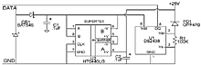
 Figure 3. A sophisticated
application of the HT0440 connects the two outputs in series
to develop a local source of ~25 V, useful as the reverse bias
voltage for photodiodes. Figure 3. A sophisticated
application of the HT0440 connects the two outputs in series
to develop a local source of ~25 V, useful as the reverse bias
voltage for photodiodes.
| | loads [3].
A more sophisticated application of the HT0440 uses the two outputs
connected in series and referenced to the voltage developed from the
parasite supply to develop a local source of ~25 V that is particularly
useful as the reverse bias voltage for photodiodes. As shown in Figure 3,
an HT0440 is connected to the parasite power generated by CR1 and C1 with
its outputs connected as just described to supply a high reverse bias
voltage for photodiode PD1. If a PIN photodiode such as the OPF470 is
used, the circuit can function as a detector sensitive to gamma radiation
[4].
Some means must then be provided to shield the sensor from optical and IR
radiation, such as by adding a metallized Mylar covering. The output
consists of random spikes generated whenever a gamma ray passing through
the diode creates a momentary increase in leakage current.
Figure 4 illustrates how the half-wave rectifier of
Figure 2 can be isolated between two addressable switches controlled by
the bus master.
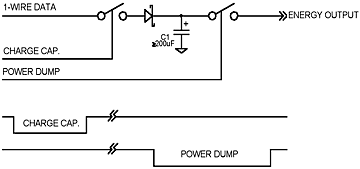
Figure 4. The half-wave rectifier in Figure 2
can be isolated between two addressable switches controlled by the
bus master.
|
When the input switch is closed, the capacitor receives charge over the
data line in the manner described above, except that because of the
greatly increased capacitance the bus must be totally dedicated to
charging the storage element during this interval and no communication is
possible. The length of the interval is a functio� of the available supply
current and the chosen capacitance value. The significant advantage of
this arrangement is that when the switch is opened, the capacitor and its
charge are isolated from the net and normal communication resumes without
the burden of leakage or capacitance loading by C1. Equally important,
isolation of the storage element and control of the energy source cycling
by the bus master prevents a capacitor/load failure from bringing down the
net. If C1 should happen to be shorted when the CHARGE CAP. switch is
closed, the DS2406 switch will revert to its default open state when its
parasite power dissipates, automatically removing the fault condition from
the main bus. When the stored energy is needed, the output POWER DUMP
switch is closed and the capacitor is discharged through the load.
Important elements of the concept and architecture are the low-level
transfer of energy from the bus master to a storage element, and the later
use of that energy in a high-energy burst. The principle is somewhat
similar to the way the circuitry used in a flash camera develops the
energy needed to fire the flashbulb.
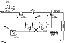
Figure 5. In this practical
example of Figure 4, a DS2406 is used as the control element
and pFETs for the switches.
| | A practical
example of this concept using a DS2406 as the control element and pFETs
for the switches is shown in Figure 5. Notice that the MIC94031 FET
isolation switches specified are 4-terminal devices with the substrate
terminal brought out. This provides for correct biasing of the terminal
under all operating conditions. The gate pull-up resistor is integral to
the chip but shown for clarity. To ensure that both switches cannot be
turned on at the same time and possibly bring down the net, a lockout
circuit is constructed using U2, a 74HC126 tri-state gate. Due to the
exclusive or connection of U2�s control pins, only alternate enabling of
the pass gates to charge and discharge the energy storage element C1 is
allowed. As shown in the truth table in Figure 5, if both outputs of the
DS2406 are inadvertently commanded to identical logic states, such as
during power up, U2 ensures that both pass gates are turned off.
In operation, C1 is charged by commanding output B (pin 6) of U1 the
DS2406 to a logic zero. This turns on Q1, connecting the data line to C1
through diode CR2, which prevents C1 from discharging back through the
net. If CR2 were not present when pass gate Q1 was turned on, and a new
slave device were to be connected on the main bus, its presence pulse
would short the net and discharge the capacitor. In the initial state with
no charge on C1, the gate of Q2 (the discharge pass gate) is held at a
higher potential than the source terminal by pull-up resistor R4, so Q2 is
off. When the bus master turns output B of U1 off, the charge stored on C1
is isolated from both the net and the load, and only leakage paths exist
to discharge it. When the bus master commands output A of U1 (pin 3) to a
logic zero, pass gate Q2 turns on and C1 discharges through the load.
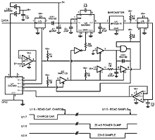
Figure 6. A barometric
pressure sensor uses a DS2450 quad A/D converter for the
1-Wire addressable switches.
| | In a practical
implementation of the concept, a barometric sensor was constructed using
U1, a DS2450 Quad ADC as the 1-Wire addressable switch control element
(see Figure 6). The DS2450 also reads the charge level of the energy
storage capacitor C1 and controls a sample-and-hold (S/H) on the output of
the sensor. A major design criterion of the circuit was that the barometer
required the energy source (C1) to provide up to 10 mA for 22 ms. In this
circuit, two of the DS2450 I/O pins are used as the digital outputs that
control the capacitor charge and discharge via analog switch U3 and a
specialized switched-capacitor voltage regulator U4 used in place of the
output (discharge) analog switch.�The charge pump, a MAX684, provides a
regulated 5 V �4% output as the energy capacitor discharges down to 2.7 V
[5]. Advantageously, the efficiency increases as the input voltage drops,
a very welcome feature when using a discharging capacitor as the energy
source. The two remaining I/O pins of U1 are used as analog inputs that
read the voltage on storage capacitor C1 and the voltage from the S/H (U7)
that stores the output from the barometer representing the current
barometric pressure. The circuit performed as expected with values up to
0.22 F for C1, the energy storage capacitor, with higher values
maintaining the output voltage constant longer. Of course, higher values
require longer charge times.
In operation, pulling U1.7 low closes analog switch U3 and allows C1 to
charge through CR1. CR1 prevents C1 from discharging back through the
1-Wire net as described previously. The voltage developed by charging C1
can be read as needed by U1.8 to ensure that there is enough energy to
operate the load. When U1.7 is turned off, analog switch U3 also turns off
and the charge stored on C1 is completely isolated from the net. At the
appropriate time, U1.6 is pulled low; this enables voltage regulator U4
and provides a path for C1 to discharge through barometer U5. The MPXA4115
requires 22 ms maximum to turn on and stabilize, after which the output
voltage representing current atmospheric pressure is stored on C3, the
sampling capacitor [6]. After sampling, U4 turns off to minimize energy
loss from storage capacitor C1. The circuit can be improved by replacing
the wide sample interval used in the prototype circuit with a narrow pulse
immediately after the output has settled.
To maximize performance, Dallas
Semiconductor recommends CAT 5 UTP (unshielded twisted pair) for the
1-Wire net. However, since CAT 5 typically comes with more than one pair,
there is a natural tendency to use a spare pair for routing power. A look
at some cable properties will help in understanding how such an
arrangement affects 1-Wire performance. In a CAT 5 cable with multiple
twisted pairs, on average any given conductor in a pair is adjacent to
another conductor in a second pair for half its length. When grounded,
this spare wire adds ~30 pF/m to the 50 pF/m between the two conductors of
a single pair. Because this increased loading reduces
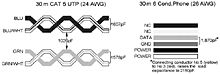
Figure 7. Shown here is the
loading effect of grounding spare conductors in the cable
using data from equal lengths of CAT 5 and 6-conductor flat
phone cable.
| | performance,
Dallas recommends that unused wires and shields be left unconnected at
both ends of the cable. The loading effect of grounding spare conductors
in the cable is detailed in Figure 7, with data taken using equal lengths
of CAT 5 and 6-conductor flat phone cable for comparison. Notice that
while capacitance between two adjacent conductors in the phone cable is
somewhat higher than in a CAT 5 pair, the effect of grounding a spare
conductor is higher with CAT 5. Still, given a relatively short 1-Wire net
with a modest number of slaves, external power can often be successfully
routed along with the data and gnd communication pair. Considera-tion must
nevertheless be given to current and voltage variations on the
power-carrying pair as they can induce crosstalk on data and gnd that
disrupts communication.
Since the bus master sees less capacitive loading over flat cable,
where the power-routing conductors are isolated from the 1-Wire bus, flat
6-conductor phone cable (Silver Satin) may be used up to about 60 m. This
assumes that DATA is separated from the power-carrying conductors by using
the outer two conductors next to the 1-Wire GND to carry power. As shown
in Figure 7, the wiring sequence should be: NC (no connection), DATA,
1-Wire GND, and then external power and ground on the two outermost
conductors. This configuration helps shield the sensitive DATA lead from
the additional capacitive load and crosstalk of the external power leads.
Notice again that the top two conductors in Figure 7 prior to the DATA
line are to be left unconnected. As previously emphasized, unless they are
left floating they will substantially increase the capacitive loading seen
by the DATA line. An alternative would be to use 4-conductor Silver Satin
and assemble the cable using 6-pin RJ-11s with these two slots in the
connector empty. Of course, this will have the effect of shifting the
1-Wire communications conductors from using the usu�l red/ green to the
yellow/green ones. Unfortunately, a significant disadvantage of flat cable
is that it lacks the noise rejection properties of twisted pair cable, so
EMI can be a significant performance problem if the net is routed near
sources of electrical noise.
A 1-Wire net consists of a
bus master communicating with multiple slaves via a single twisted-pair
cable over which they also receive operating power. While the fusion of
network connection and power provides for great economy, the question of
how to provide energy for the occasional indicator or sensor is often
raised. Common examples include operating an LED indicator and providing
high-voltage bias for a photodiode or moderate current for a pressure
sensor. Unless local power is in place, or running a separate cable is an
option, some means of transferring these energy requirements over the same
1-Wire communication bus is required. This article has reviewed several
ways to provide this energy over the communications twisted pair as well
as recommendations for using spare conductors in the cable.
1-Wire and 1-Wire net are trademarks of Dallas
Semiconductor.
1. �EA
HREF="http://www.ibuttonlink.com" TARGET="_blank">The LINK.�E/P>
2. Awtrey, Dan, �EA HREF="/articles/0698/wir0698/" TARGET="_top">The
1-Wire Weather Station,�ESensors, June 1998, pp. 34�E0.
3. The HT0440 data sheet.
4. The OPF470 data sheet.
5. The MAX684 data sheet.
6. The MPXA4115 data sheet.
Parts
List
|
(in
order of mention in the text)
|
DS2406, DS2480, DS9097U, DS2423, DS2450,
MAX684
Dallas
Semiconductor
(Maxim)
Sunnyvale,
CA
408-737-7600
BAT54S
Fairchild
Semiconductor
South Portland,
ME
207-775-8100
800-341-0392 (outside
Maine)
800-832-5505 (inside Maine)
HT0440
Supertex
Inc.
Sunnyvale, CA
408-222-8888
|
OPF470
ChipDocs.com
Digi-Key.com
Pacer
Components
MIC94031
Micrel
San
Jose, CA
408-944-0800
74HC126
Philips Logic
Eindhoven, The
Netherlands
MPXA4115
Motorola
CAT 5 UTP
Cat 5
Cable Co.
Sherwood,
AR
866-835-2285
| |
Dan Awtrey is an
independent consultant, Dann EL Associates, Garland, TX; mailto:dawtrey@%20comcast.net.
|

|